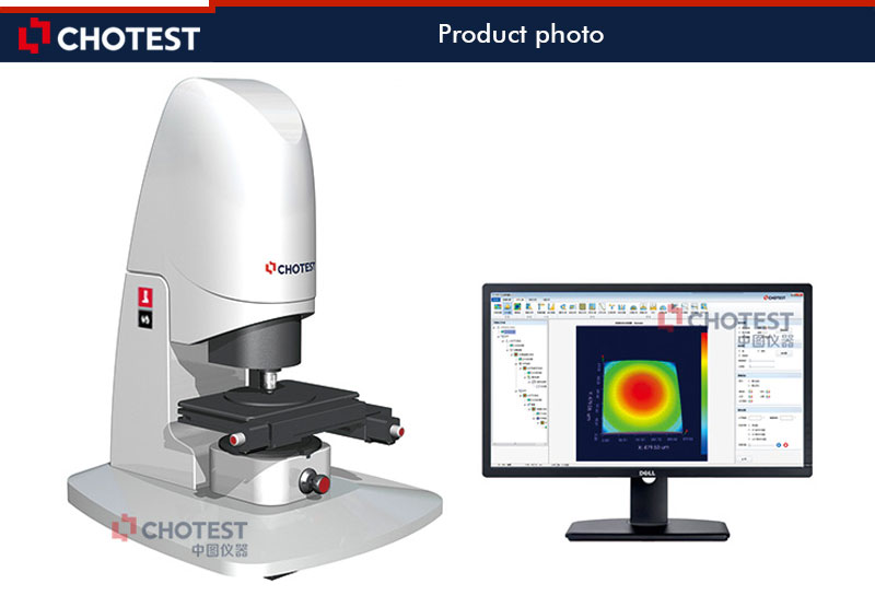
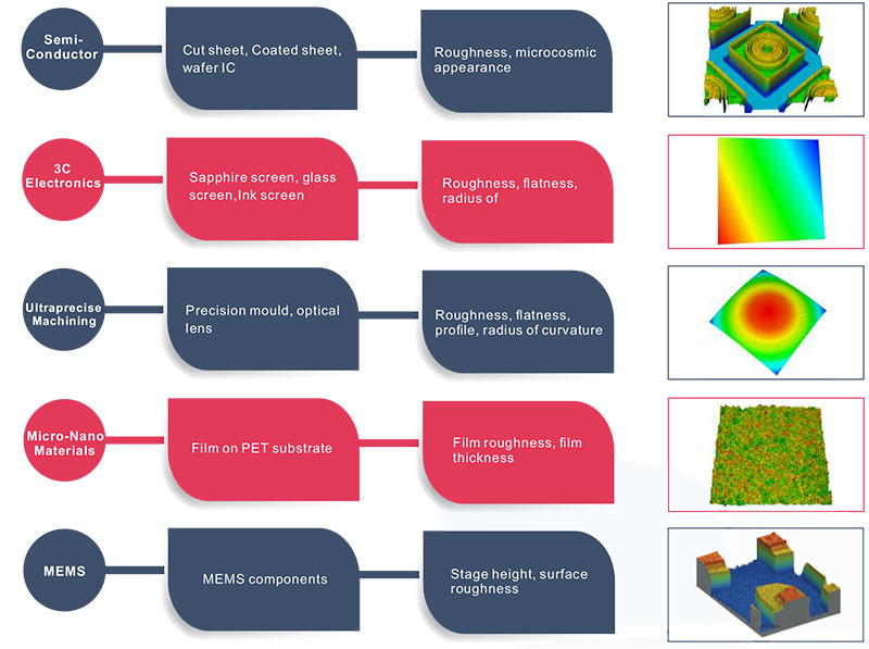
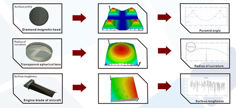
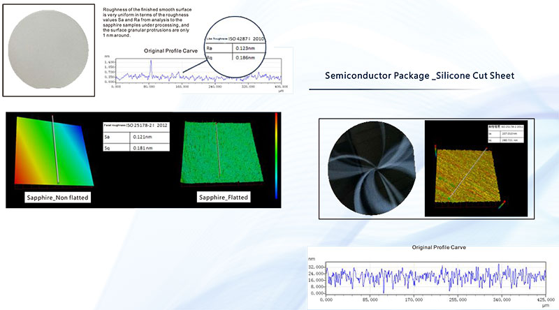
There are 1 rough roughness profilome from 1 suppliers on EC21.com
Related Searches : optical instrument , motorized stages , translation stages , rotation stages
Price
1 - 9
US$ 10≥10
US$ 1Supplier Info.
Report Item
Your report on Product(s) will be sent to EC21 Administrators once submitted.
Then, Administrators will investigate and then take appropriate actions.
Contact Supplier
SuperView W1 Optical 3D Surface profilometer is an ideal instrument for sub-Nanometer measurement of various precision parts. Based on the principle of white light interference technology, combined with precision Z-direction scanning module and 3D modeling algorithm, it contactlessly scans the surface of the object then establish a 3D image for the surface. A serial of 2D, 3D parameters reflecting surface quality of the object are obtained after XtremeVision software processes and analyzes the 3D image. The SuperView W1 is a user-friendly precision optical instrument with powerful analysis functions for all kinds of surface form & roughness parameters. With unique light source it could measure various precision parts with both smooth and rough surface.

| Model No. | SuperView W1 | SuperView W1-Pro | |
| Light source | White LED | ||
| Video system | 1024×1024 | ||
| Standard Field of View | 0.98×0.98 mm | ||
| Max Field of View | 6.0×6.0 mm(Optional) | ||
| Lens Turret | Manual 3 holes turret(Optional: Motaorized 5 holes turret) | ||
| XY Object table | Size | 320×200mm | 300×300mm |
| Moving range | 140×100mm | 200×200mm | |
| Loading capacity | 10kg | ||
| Control method | Motorized | ||
| Tilt | ±5° | ||
| Z Axis | Tracvel range | 100mm | |
| Control method | Motorized | ||
| Z Stroke Scanning range | 10mm | ||
| Surface Form Repeaability*2 | 0.1nm | ||
| Roughness RMS Repeatability*3 | 0.005nm | ||
| Step Hiehgt Measurementy*4 | Accuracy: 0.3% Repeatability: 0.008%(1σ) | ||
| Scanning Speed at 0.1nm resulution | 1.85μm/s | ||
| Reflectivity of Test Object | 0.05%~100% | ||
| Size(L*W*H) | 700x606x920mm | ||
| Weight | <160kg | ||
| Operating Environment | Temperature | 15°C~30°C, fuctuation <1°C/15min | |
| Humidity | 5%~95% RH, no condensation | ||
| Vibration | VC-C or better | ||
| Software Noise Evaluation*5 | 3σ≤4nm | ||
| Compressed Air | 0.6Mpa oil-free, water-free, 6mm diameter of hose | ||
| Power Supply | AC100~240V, 50/60Hz, 4A, 300W | ||
| Other | No strong magnetic field, No corrosive gas | ||
| *1 W1 is the standard model of 3D Optical Surface Profilometer; W1-pro has larger stage size and travel range. W1-Ultra has greatly improved the scanning speed compared to W1. *2 Use EPSl mode to measure Sa 0.2nm silicon wafer in the laboratory environment; Single stripe, 80um filter for full field of view *3 Measure Sa 0.2nm silicon wafer in a laboratory environment according to the ISO 25178. *4 Measure standard 4.7μm steps height block in a laboratory environment according to the ISO 5436-1:2000 *5 When the software noise evaluation is 4nm≤3σ≤10nm, the Roughness RMS repeatability is revised down to 0.015nm, the Step height measurement accuracy is revised down to 0.7%, and the step height measurement repeatability is revised down to 0.12%; When the software noise evaluation is 3σ>10nm, the environment does not meet the requirement for usage of the equipment, and need to change the site. |
|||
Remark: Performance parameters are tested by using a 4.7µm precision master stage gauge in lab according to ISO 4287 and ISO 25178.
|
Zoom ratio of lens |
2.5× |
5× |
10× |
20× |
50× |
100× |
||
|
Numerical hole diameter |
0.075 |
0.13 |
0.3 |
0.4 |
0.55 |
0.7 |
||
|
Optical resolution at 550nm (µm ) |
3.7 |
2.1 |
0.92 |
0.69 |
0.5 |
0.4 |
||
|
Depth of focus( µm) |
48.6 |
16.2 |
3.04 |
1.71 |
0.9 |
0.56 |
||
|
Working distance( mm) |
10.3 |
9.3 |
7.4 |
4.7 |
3.4 |
2.0 |
||
|
Field H ×V (mm) |
Video system 1024×1024 |
0.5× |
3.92× 3.92 |
1.96×1.96 |
0.98×0.98 |
0.49×0.49 |
0.196×0.196 |
0.098×0.0 98 |
|
0.75× |
2.6× 2.6 |
1.3×1.3 |
0.65×0.65 |
0.325×0.325 |
0.13×0.13 |
0.065×0.065 |
||
|
1× |
1.96× 1.96 |
0.98×0.98 |
0.49×0.49 |
0.245×0.245 |
0.098×0.098 |
0.049 ×0.049 |
||
※ Built-in ISO/ASME/EUR/GBT Standards of 2D, 3D parameters:
2D Parameters
|
Standard |
Parameters |
|||
|
ISO 4287-1997 |
Principal section |
Roughness |
Waviness |
|
|
Amplitude |
Pp, Pv ,Pz, Pc, Pt,Pa,Pq,Psk,Pku |
Rp, Rv ,Rz, Rc, Rt,Ra,Rq,Rsk,Rku |
Wp, Wv ,Wz, Wc, Wt,Wa,Wq,Wsk,Wku |
|
|
interval |
PSm,Pdq |
RSm,Rdq |
WSm,Wdq |
|
|
Substance |
Pmr,Pdc |
Rmr,Rdc,Rmr(Rz/4) |
Wmr,Wdc,Wmr(Wz/4) |
|
|
Peak |
PPc |
RPc |
WPc |
|
|
ISO 13565 |
ISO 13565-2 |
Rk,Rpk,Rvk,Mr1,Mr2,A1,A2,Rpk,Rvk |
||
|
ISO 12085 |
Roughness graph |
R,AR,R× ,Nr |
||
|
Waviness graph |
W,AW,W×,Wte |
|||
|
Other graph |
Rke,Rpke,Rvke |
|||
|
AMSE B46.1 |
2D |
Rt,Rp,Rv,Rz,Rpm,Rma×,Ra,Rq,Rsk,Rku,tp,Htp,Pc,Rda,Rdq,RSm,Wt |
||
|
DIN EN ISO 4287-2010 |
Original profile |
Pa,Pq,Pp,Pv,Pz,Pc,Pt,PSk,PKu,PSm,PPc,Pdq,Pdc,Pmr, |
||
|
Roughness |
Ra,Rq,Rp,Rv,Rz,Rc,Rt,RSk,RKu,RSm,RPc,Rdq,Rdc,Rmr, |
|||
|
Waviness |
Wa,Wq,Wp,Wv,Wz,Wc,Wt,WSk,WKu,WSm,WPc,Wdq,Wdc,Wmr |
|||
|
JIS B0601-2013 |
Original profile |
Pa,Pq,Pp,Pv,Pz,Pc,Pt,PSk,PKu,PSm,PPc,Pdq,Pdc,Pmr, |
||
|
Roughness |
Ra,Rq,Rp,Rv,Rz,Rc,Rt,RSk,RKu,RSm,Rdq,Rdc,Rmr |
|||
|
Waviness |
Wa,Wq,Wp,Wv,Wz,Wc,Wt,WSk,WKu,WSm,WPc,Wdq,Wdc,Wmr |
|||
|
GBT 3505-2009 |
Original profile |
Pa,Pq,Pp,Pv,Pz,Pc,Pt,PSk,PKu,PSm,PPc,Pdq,Pdc,Pmr, |
||
|
Roughness |
Ra,Rq,Rp,Rv,Rz,Rc,Rt,RSk,RKu,RSm,Rdq,Rdc,Rmr |
|||
|
Waviness |
Wa,Wq,Wp,Wv,Wz,Wc,Wt,WSk,WKu,WSm,WPc,Wdq,Wdc,Wmr |
|||
3D Parameters
|
Standard |
Parameters |
|
|
ISO 25178 |
Height |
Sq,Ssk,Sku,Sp,Sv,Sz,Sa |
|
function |
Smr,Smc,S×p |
|
|
Space |
Sal,Str,Std |
|
|
Composite parameters |
Sdq,Sdr |
|
|
Volume |
Vm,Vv,Vmp,Vmc,Vvc,Vvv |
|
|
Form |
Spd,Spc,S10z,S5p,S5v,Sda,Sha,Sdv,Shv |
|
|
Functional |
Sk,Spk,Svk,Smr1,Smr2,Spq,Svq,Smq |
|
|
ISO 12781 |
Flatness |
FLTt,FLTp,FLTv,FLTq |
|
EUR 15178N |
Amplitude |
Sa,Sq,Sz,Ssk,Sku,Sp,Sv,St |
|
Space |
Str,Std,Sal |
|
|
Composite parameters |
Sdq,Sds,Ssc,Sdr,Sfd |
|
|
Area, Volume |
Smr,Sdc |
|
|
Function |
Sk,Spk,Svk,Sr1,Sr2,Spq,Svq,Smq |
|
|
Functional |
Sbi,Sci,Svi |
|
|
EUR 16145 EN |
Amplitude |
Sa,Sq,Sy,Sz,Ssk,Sku |
|
Mixed parameters |
Ssc,Sdq,Sdr |
|
|
Functional |
Sbi,Sci,Svi,Sk,Spk,Svk |
|
|
Space |
Sds,Std,Stdi,Srw,Srwi |
|
|
Hardness |
Hs,Hvol,Hv,Hps,Hpvol,Hpv,Hap,Hbp |
|
|
ASME B46.1 |
3D |
St,Sp,Sv,Sq,Sa,Ssk,Sku,SWt |
It is used for measurement and analysis of surface roughness and profile of precision components from industries of semi-conductor, 3C Electronics, ultraprecise machining, optical machining, micro-nano materials, micro-electro-mechanical system.

Measurement and analysis for various products, components and materials`surface form and profile characteristics, such as flatness, roughness, waviness, appearance, surface defect, abrasion,corrosion, gap, hole, stage, curvature, deformation, etc.

3C Electronics_Sapphire crystal

3C Electronics _ Ink screen


| Registration Date | 2024/06/13(Year/Month/Date) |
|---|---|
| Buyer / Seller in EC21 | Seller |
| Business Type | Manufacturer |
| Year established | 2005 |
| Employees total | 501 - 1000 |
| Annual revenue | USD 500,001 - 1,000,000 |
| Company | CHOTEST Technology Inc. |
|---|---|
| Address | 2/F, Building B1, Zhiyuan, Xueyuan Road, Xili, Nanshan, Shenzhen 518071, ChinaShenzhenGuangdong518000China |
| Phone | 86 - 83318988 - 227 |
| Homepage | en.chotest.com |
| Contact | Omiga |